A University of São Paulo (USP) presented this Tuesday (16), the PocketFabannounced as the first portable, modular and sustainable semiconductor factory in the world, at an event at 3pm at Espaço Iris, with the aim of putting Brazil on the global chip production map through an innovative model that combines technological autonomy, sustainability and democratization of access to advanced microelectronics.
Read more:
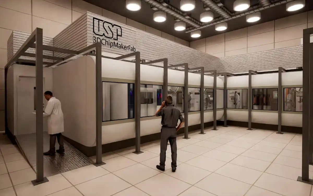
Compact and reconfigurable factory
Developed at InovaUSP in cooperation with the Federation of Industries of the State of São Paulo (Fiesp) and the National Service for Industrial Learning (Senai), PocketFab condenses all the functions of a semiconductor pilot line into a compact and reconfigurable infrastructure. The proposal allows universities, startups and industrial partners to access advanced manufacturing processes without needing the billion-dollar investments required by traditional factories.

In practice, PocketFab brings together the main steps for manufacturing and assembling chips into integrated modules. These include additive micromanufacturing, similar to 3D printing of electronic components on a microscopic scale, lithography and metallization processes to design circuits, and heterogeneous packaging, which combines different chiplets into a single, more powerful system. The structure also has clean room modules, testing and metrology stations.
5D glass memory promises to last 13.8 billion years and store 360 TB on a 5-inch disk
With this configuration, PocketFab can develop everything from three-dimensional microprocessors for artificial intelligence to internet of things (IoT) devices, microelectromechanical and optical components (MOEMS) and environmental sensors capable of monitoring CO₂, weather conditions and pollution. The total investment in the initiative was not disclosed by the university.
Viable economic model
According to Marcelo Zuffo, director of InovaUSP, PocketFab arises from an economic and technological analysis of the sector. Traditional chip factories are large, expensive structures that require billion-dollar investments with long payback periods. USP’s bet is to apply a downsizing process to the industry, reducing scale and costs to make manufacturing accessible and compatible with university environments and innovation centers.
The model works as a pilot line capable of processing around 20 wafers per day in its initial configuration. Each wafer can generate thousands of chips, depending on the size of each component. Zuffo explains that the objective is to concentrate more stages of the production process in a modular set, from the wafer to the final chip, reducing external dependencies and creating local manufacturing capacity.
“We managed to do it for a value that is practically one hundredth of the price of a conventional factory“, says Zuffo. He admits that production capacity is also reduced in the same proportion, but sufficient to start continuous chip manufacturing and demonstrate viability. In a country that imports between US$40 billion and US$50 billion in technology per year and exports a fraction of that, the director sees the initiative as a way to expand local processing and export potential.
Ambitious scientific agenda
In addition to the industrial aspect, PocketFab aims for an ambitious scientific agenda. The infrastructure will make it possible to advance the development of chips for artificial intelligence and quantum computing, exploring the convergence between these areas. For Zuffo, this is an attempt to reposition Brazil in a strategic field whose evolution is accelerated and central to the global technological dispute, placing the country in the club of nations that own this technology.
Environmental sustainability
Another central axis of the initiative is environmental sustainability. PocketFab was designed to reduce energy, water and chemical consumption, in addition to requiring smaller clean room areas. The model paves the way for future “green chip” certification, aligning microelectronics with environmental and climate goals in a sector traditionally intensive in natural resources.
The modular and portable architecture makes PocketFab one of the first semiconductor factory concepts of its kind in the Southern Hemisphere. It can be installed in universities, technology parks, industrial districts or regions where conventional factories would be unfeasible. Zuffo compares the model to the logic of bakeries: instead of a few concentrated giant plants, scale would come from the multiplication of smaller, replicable units.
Global crisis context
PocketFab appears at a time of global reevaluation of semiconductor chains. The fragility of the concentrated model became evident from 2020 onwards, when the pandemic led to the closure of factories in Asia, responsible for the majority of global production. The mismatch between supply and demand created a prolonged bottleneck that affected entire production chains, consolidating the perception that semiconductors are a critical factor in economic security.
Source: Estadão

Join the Adrenaline offer group
Check out the main offers on hardware, components and other electronics that we found online. Video card, motherboard, RAM memory and everything you need to build your PC. By joining our group, you receive daily promotions and have early access to discount coupons.
Join the group and take advantage of promotions
Source: https://www.adrenaline.com.br/hardware/usp-anuncia-projeto-de-fabrica-portatil-de-semicondutores-para-o-pais/