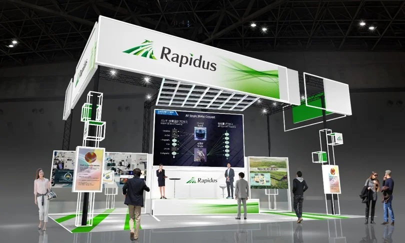
The Japanese company Rapidus has invested a lot – with the help of more companies and government subsidies – to become a real competitor to TSMC in the advanced chip segment. And now the Japanese giant is preparing to discuss a technology that can help it take a leap and get ahead of its competitors.
Today, December 17th, the 2025 edition of SEMICON Japan begins, an international event for semiconductor technology companies, based in the Asian country. During the show, Rapidus plans to offer details on how it is working on joining panel-level packaging (PLP) with glass substrates in one go.
These are two of the technologies that are still in the early stages of development in the laboratories of many companies involved with semiconductors – including TSMC itself. But Rapidus seems confident that it will be able to arrive first at the moment when it will be possible to combine the two processes.
Glass substrates are the next big step for processors
Currently, most processors, including the most advanced, are based on silicon wafers placed in packages of organic substrates. While silicon supports high circuit density and precise dimensional control, substrates do not support these same properties, so we are approaching the limit of what the material can offer in cutting-edge technologies.

Glass substrates, in turn, bring much more advanced properties suitable for chip manufacturing, in addition to withstanding much higher operating temperatures. These are all especially important advantages in the fast-paced AI and HPC segment, which requires increasingly scalable servers that operate at elevated temperatures.
AMD is another example of a company working on substrates, while Intel also had plans but reportedly gave up. Rapidus’ efforts in the area appear more recent.
PLP is already used in chips, but Rapidus wants to join new substrates
Panel-level packaging allows chips to be packaged in large rectangular panels instead of the traditional round wafers we are used to seeing. In the case of Rapidus, they would be 600 x 600mm panels.
This allows for more efficient manufacturing, with greater component yield, in larger packages. FOPLP (Fan-Out Panel-level Packaging) is already used in simpler chips, but we do not yet have advanced processors produced at a commercial level with PLP packaging.
Read more:
That’s why Rapidus wants to take advantage by immediately delivering the first chips with glass substrates already packaged in PLP. Obviously there is a huge difference between forecasts and practical deliveries, but this could be the Japanese company’s chance to jump ahead of rival semiconductor manufacturers.
Via: Tom’s Hardware

Join the Adrenaline offer group
Check out the main offers on hardware, components and other electronics that we found online. Video card, motherboard, RAM memory and everything you need to build your PC. By joining our group, you receive daily promotions and have early access to discount coupons.
Join the group and take advantage of promotions
Source: https://www.adrenaline.com.br/hardware/rapidus-quer-atravessar-concorrentes-e-ja-fala-em-chips-com-substratos-de-vidro-e-plp/