Researchers from several American universities and a commercial foundry in the United States have announced a landmark innovation in semiconductor technology: the development of what is described as the first truly three-dimensional (3D) chip produced in a commercial chip factory.
The prototype combines memory and logic on a single silicon wafer, using transistors based on carbon nanotubes and RRAM memory layers, which can pave the way for significant gains in performance and efficiency in hardware aimed at artificial intelligence and other advanced applications.
What does a real three-dimensional chip mean?
Traditional semiconductor architecture is two-dimensionalwith components positioned side by side on the surface of the chip.
In the new design, the processing logic and memory cells are stacked vertically on a single wafer, increasing the density of connections and shortening the communication paths between processing and data units.
The method surpasses previous “3D packaging” solutions in which multiple chips were integrated into the same package; here, the layers are created sequentially on the same integrated circuit, which characterizes a true monolithic three-dimensional integrated circuit.
How was the prototype produced?
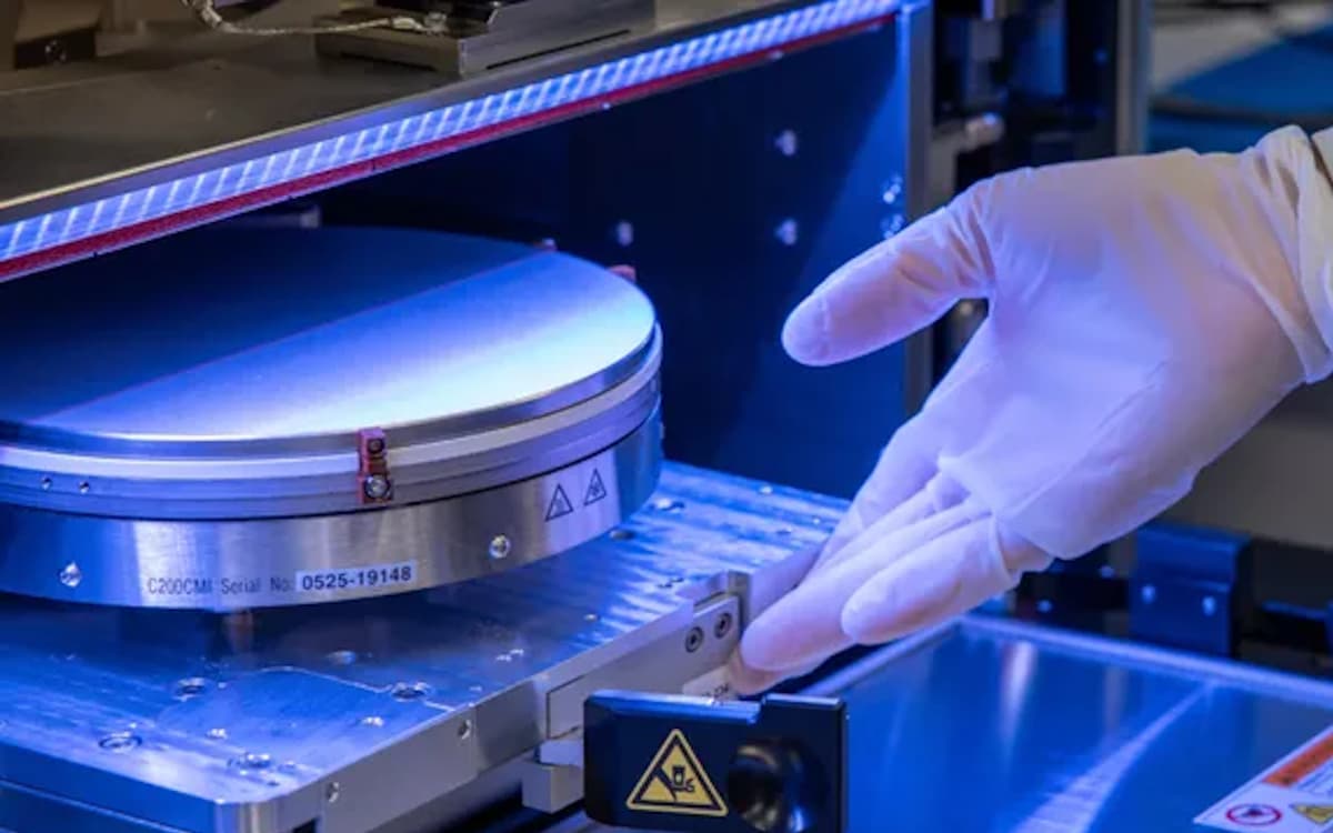
The chip was manufactured in the company’s commercial production process. SkyWater Technologya foundry located in the United States known for operating in mature technology from 90 nm to 130 nm.
The manufacturing used a low temperature process (about 415 °C) to prevent damage to the bottom layer of circuits while successive layers were added.
In this way, the process allowed integration into a single chip field effect transistors with carbon nanotubesresistive non-volatile memory (RRAM) and traditional silicon CMOS logic, with a dense network of vertical interconnects that significantly reduce signal distance between components.
Results in tests and simulations
When compared to a traditional flat-design chip operating with similar latency and area, the prototype showed performance gains of approximately four times in throughput in real hardware tests.

Additionally, through simulations with higher memory and compute stacks, the research group observed up to twelve times more performance on typical desktop workloads artificial intelligenceincluding models derived from the architecture of large language models.
The researchers also estimate that as vertical integration continues to expand, this approach could result in improvements between 100 times and 1 000 times in the energy-delay product — a metric that combines energy efficiency and speed — compared to conventional 2D architectures.
Designs with additional layers show potential for improvements between 100 times and 1000 times in the energy-delay productwhich combines energy efficiency and speed, as vertical integration is expanded beyond current prototypes
Participation of universities and industry
The development of the chip involved engineers and scientists from Stanford University, Carnegie Mellon University, University of Pennsylvania e MITin partnership with SkyWater Technology, which transformed the academic research concept into a prototype manufactured in an industrial environment.
Collaboration between academia and industry is seen as an important step towards demonstrating that so-called architectures 3D monolithic they can be produced outside of specialized laboratories and migrate to reliable production lines used by the semiconductor industry.
Step beyond conventional chips
Subhasish Mitra, professor of electrical engineering and computer science at Stanford and principal investigator on the project, commented that the transition from an academic concept to a chip manufactured in a commercial foundry opens doors to a new era of semiconductor productionwith the potential to meet the future demands of AI systems and high-intensity computing.
Vertical integration can be understood as an evolution of semiconductor performance strategies, which historically rely on the miniaturization of transistors in two-dimensional planes.
By utilizing the third dimension, engineers hope to reduce internal communication bottlenecks and overcome physical limitations that traditional architecture faces today.
Where can this technology go?
Although the prototype is still at an early stage, the results indicate that monolithic 3D chips with carbon nanotubes and integrated memory could offer paths for devices with processing density and energy efficiency much higher than current options.
This is welcome in applications such as AI accelerators, high-performance embedded systems and equipment that demand a combination of large volumes of data and low energy consumption.
Also read:
The future of chip production
By combining nanotechnology, advanced memory and vertical integration on a single chip, researchers and manufacturers show that New semiconductor architectures may emerge as viable alternatives on an industrial scaleinfluencing hardware design for decades to come.
Thus, perhaps the traditional performance limits imposed by 2D architecture can be reevaluated and the local production of chips with innovative architectures can gain strategic relevance in a global context of accelerated technological competition.
Source: Stanford University
Source: https://www.adrenaline.com.br/hardware/chip-3d-nanotubos-carbono-ram-integrada/