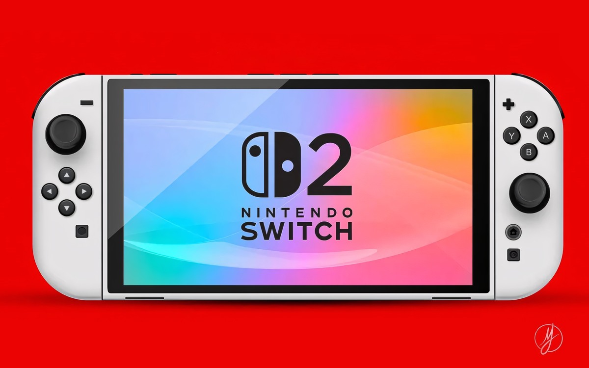
Even today (Monday, 6th) the Digital Foundryin their weekly podcast episode, commented on the potential leak of the Nintendo Switch 2 motherboard. They argue that there is a very high probability of chip is 8nm made by Samsungwhich generates efficiency concerns. However, we still need to see how NVIDIA and Nintendo have adapted the hardware for the hybrid.
Leaked information about the possible architecture of the Nintendo Switch 2 indicates that the console could be powered by a chip T239manufactured by Samsung in a process of 8 nm.
While this choice may pose challenges related to performance and battery life, experts at Digital Foundry suggest it could be a balanced solution considering Nintendo’s efficiency and cost goals.
Reasons for choosing Samsung’s 8nm process for the Nintendo Switch 2
The T239 chip, developed by NVIDIA, derives from the architecture Ampereoriginally designed for 8nm processes.
One of the main arguments for imagining that Samsung’s 8nm chips would be used in the Switch 2 is precisely that adaptations to more advanced technologies, such as 5nm or 4nm, would require considerable investment for portability to Ampere, which would imply additional costs and development times.
At the moment, there is no guarantee that it is actually Samsung 8nm, but the evidence is leaning towards that. There has been some conjecture that it’s possibly Samsung 5nm, which, you know, can’t be ruled out. But then again, why would you port Ampere to this? It’s a little strange.
In other words, if they wanted to migrate to 4nm, it would make more sense if NVIDIA opted for the Lovelace architecture, which was already designed for this manufacturing process without relying on a complex porting process.

The choice of 8nm appears to align with Nintendo’s approach of prioritizing cost-effective and stable hardware solutions. Samsung’s 8nm process is cost-effective, in part due to its lower popularity and current low demand, making it affordable for large-scale projects like the Switch 2.
Potential performance and battery impacts
Although the 8nm process is not known for its energy efficiency, there are factors that can mitigate potential negative impacts.

Preliminary comparisons indicate that the T239 may offer improved thermal performance and power consumption over the T234 on which it is based. This is because the T239 is smaller it was probably optimized for different uses than the original chips.
My sources say that although the T239 was created as an offshoot of the T234, they were designed by separate teams and pretty much the only thing they have in common is the Ampere architecture. The CPU is different. There is a file decompression block for the console, which is necessary for fast loading and fast asset management. So it is indeed a very different product. It’s not really a scaled-down T234. And if it was designed from scratch for the 8 nanometer process, you have to understand that NVIDIA engineers probably know what they’re doing. They would have designed the product for this process. They would have specific energy efficiency goals in mind.
It is also worth highlighting that, even with efficiency limitations, the Switch 2 can benefit from exclusive features provided by the use of NVIDIA technology. Support for DLSS (Deep Learning Super Sampling) is one of these advantages.
While experts and fans discuss the possibilities of what the Nintendo Switch 2 can deliver and speculation continues, we still need official confirmation and a full announcement from Nintendo to be sure what the device will be.
As always, it’s worth listening to the full discussion in the original Digital Foundry video to better understand the details.
Leaked and rumored Nintendo Switch 2 specs
The table below was put together based on information shown in the leaked photo of the device’s motherboard, with other information also from recurring rumors.
All information is rumors, and will not be completely confirmed until an official announcement of the new console by Nintendo.
| Component | Specification |
| Architecture | ARM Cortex |
| APU | NVIDIA Tegra T239 |
| SoC CPU | Not confirmed; ARM-based. |
| SoC GPU | NVIDIA Ampere, 1536 CUDA cores. |
| RAM memory | 12GB LPDDR5X, 7500 MT/s. |
| Internal Storage | 256GB UFS 3.1 (Kioxia). |
| Bodies | 8″, probably 1080p |
| Battery | Possibly 20Wh. |
| Weight | Not confirmed. |
| Dimensions | 27.0 x 11.6 x 1.4 cm. |
| Connectivity | Wi-Fi e Bluetooth (MT3681AEN). |
| Operating System | Customized by Nintendo. |
| USB Controller | Genesys Logic GL852G, USB 2.0 para Joy-Cons. |
| Cartridge Reader | MegaChips B2349; backwards compatible with old cartridges. |
| Memory Controller | PI2SSD 3212NCE, optimized for new cartridges. |
| Audio Chip | Realtek ALC5658 |
| NFC reader | PN7160B1HN/C100 for amiibos. |
| USB-C Controller | CYPD6228-96BZXI, for charging and accessories. |
| SD Card Reader | Expected support for SD Express. |
Source: Digital Foundry.

Join the Adrenaline offer group
Check out the main offers on hardware, components and other electronics that we found online. Video card, motherboard, RAM memory and everything you need to build your PC. By joining our group, you receive daily promotions and have early access to discount coupons.
Join the group and take advantage of promotions
Source: https://www.adrenaline.com.br/games/nintendo/nintendo-switch-2-chip-de-8nm-da-samsung-pode-ser-uma-estrategia-de-reducao-de-custo-aponta-digital-foundry/


